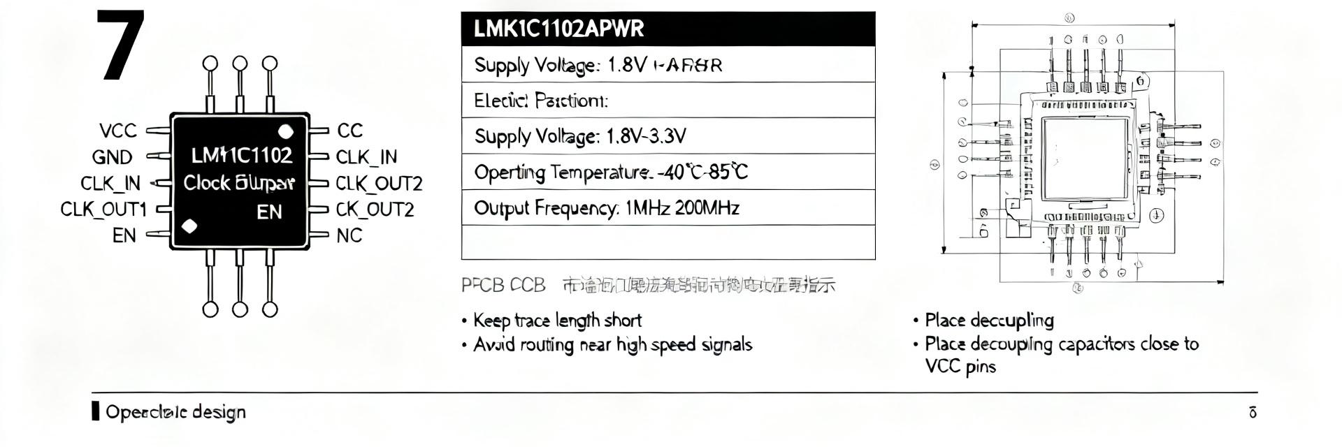
In 5G base stations, data centers, and industrial automation, clock signal integrity directly determines system performance. As a 4-channel LVCMOS clock buffer launched by Texas Instruments (TI), LMK1C1104APWR has become the preferred device for high-frequency clock distribution schemes due to its core specifications of <50ps output skew and <50fs additive jitter. Based on the latest official datasheet, this article deeply analyzes its electrical characteristics, package details, and engineering selection keypoints to help you quickly complete design validation.
Core Architecture and Functional Positioning
1:4 LVCMOS Buffer Design Principle
The LMK1C1104APWR adopts a fan-out architecture to distribute a single-ended clock input to 4 independent outputs. The core circuit integrates an input buffer stage, a clock tree distribution network, and an output driver stage, ensuring signal integrity through internal matching networks. The device supports clock frequencies up to 200MHz, meeting the timing requirements of high-speed interfaces such as Gigabit Ethernet and PCIe Gen3.
The key design advantage is reflected in full voltage rail compatibility—it can directly interface with 1.8V, 2.5V, or 3.3V systems without level translation circuits, significantly simplifying the power supply architecture. The output driver stage adopts a push-pull structure, providing a 24mA drive capability to drive long-distance PCB traces or multi-load scenarios.
Multi-Scenario Applications: Communication, Computing, and Industry
In the field of communication infrastructure, this device provides low-jitter reference clock distribution for FPGAs and ASICs; in server and data center applications, it supports the construction of multi-channel processor synchronous clock trees; in industrial automation scenarios, its wide operating temperature range (-40°C to +85°C) ensures reliability in harsh environments. The versatility across three sectors stems from its product philosophy of 'uncompromised performance, simplified design'.
In-Depth Interpretation of Electrical Characteristics
Power Supply Voltage Range: 1.8V/2.5V/3.3V Fully Compatible Design
The device supports a continuous power supply range from 1.65V to 3.6V, with core parameters dynamically optimized with voltage. At 1.8V supply, the quiescent current is only 2.5mA, and under 3.3V supply, the output rise time is shortened to 1.5ns. It is recommended to use an independent power plane and achieve decoupling through a combination of 0.1μF+10μF ceramic capacitors to suppress high-frequency noise coupling.
Key Timing Parameters: Propagation Delay, Output Skew, and Jitter Performance
The typical propagation delay is 3.5ns (3.3V/15pF load), and the channel-to-channel output skew is <50ps, ensuring phase consistency across multiple clocks. The additive jitter specification is particularly outstanding: <50fs within the 12kHz to 20MHz integration bandwidth, far exceeding competing products. This performance directly determines the bit error rate (BER) margin of high-speed serial links, making it an ideal choice for SerDes clock distribution.
| Parameter | Test Conditions | Typical | Maximum |
|---|---|---|---|
| Propagation Delay | 3.3V, 15pF | 3.5ns | 5.0ns |
| Output Skew | Same Edge | — | 50ps |
| Additive Jitter | 12kHz - 20MHz | 35fs | 50fs |
| Rise/Fall Time | 20% - 80% | 1.5ns | 2.5ns |
Input/Output Level Standards and Drive Capability
The input is compatible with LVCMOS/LVTTL levels, with threshold voltages at 30%/70% of the power supply voltage. The output swing features a rail-to-rail design, with a high level of ≥2.9V (IOH=-24mA) and a low level of ≤0.4V (IOL=24mA) at 3.3V supply. It is recommended to connect a 22Ω damping resistor in series at the output to suppress signal reflections.
Package Parameters and PCB Layout Keypoints
TSSOP-8 Package Dimensions and Pin Definition Detailed
It adopts a 3.00mm × 3.00mm TSSOP-8 package with a pin pitch of 0.65mm and a height of 1.10mm. The pin assignment follows the general specifications of clock buffers: Pin 1 CLKIN is a single-ended input, Pins 2-5 Y1-Y4 are non-inverting outputs, Pin 6 OE is the enable control (active high), and Pins 7-8 are power and ground. The compact package fits space-constrained, high-density PCB designs.
Thermal Performance and Heat Dissipation Design Recommendations
The typical thermal resistance θJA is 180°C/W (JEDEC standard 4-layer board). Under continuous operating conditions, the junction temperature must be controlled within 125°C. It is recommended to place a thermal via array under the device to connect to the inner ground plane; for high power consumption scenarios, the exposed pad (EP) version can be considered to enhance heat dissipation.
Layout and Routing: Clock Trace Impedance Control and Termination Strategy
The clock input trace should preferentially use a 50Ω microstrip line or a 100Ω differential pair (if a differential source is used), with the length controlled within 2.5cm. The four output traces must be strictly matched to equal length with a deviation of <2.5mm to maintain the skew specification. Avoid routing clock lines across power split planes, and add ground return vias if necessary. The output termination scheme is selected based on the load type: series termination at the source for a single load, and Thevenin or AC termination for multiple loads.
Selection Comparison and Alternative Solutions
LMK1C110x Series Horizontal Comparison (1102/1103/1104/1106/1108)
| Part Number | Output Channels | Package | Typical Application |
|---|---|---|---|
| LMK1C1102 | 2 channels | SOT-23-6 | Simple Clock Distribution |
| LMK1C1103 | 3 channels | TSSOP-8 | Small-scale Systems |
| LMK1C1104APWR | 4 channels | TSSOP-8 | General High-Speed Distribution |
| LMK1C1106 | 6 channels | TSSOP-14 | Complex Clock Trees |
| LMK1C1108 | 8 channels | TSSOP-16 | Large-scale Systems |
The core basis for selection is the requirement for the number of output channels and PCB area constraints. The four-channel version achieves the best balance in performance-density ratio and is the default choice for most medium-scale systems.
Competing Product Parameter Benchmarking: Domestic Alternative Feasibility Assessment
Domestic manufacturers such as SGMICRO and 3PEAK have introduced pin-compatible clock buffer series. The comparison shows that domestic devices are close to international levels in basic electrical parameters, but there is still a generational gap in <100fs level jitter performance. For non-ultra-high-speed applications (≤100MHz), domestic solutions offer cost advantages; for scenarios like 5G fronthaul and high-end computing, it is recommended to prioritize the original TI devices to ensure margin.
Typical Application Circuits and Debugging Guide
Single-Ended Clock Distribution Reference Design
The standard application circuit includes: an input RC filter network (optional, to suppress high-frequency spurs), the device itself, output series resistors, and load capacitors. The power pin is configured with a 0.1μF ceramic capacitor close to it for decoupling, and the enable pin is pulled up to VCC or connected to an MCU for dynamic control. Complete design files can be obtained from official channels.
Common Troubleshooting: Signal Integrity Optimization Tips
If the measured skew exceeds the specification, first check the output trace length matching and load symmetry; jitter degradation usually stems from power supply noise or input signal quality, and it is recommended to use a spectrum analyzer to troubleshoot power supply ripple; output ringing issues can be resolved by adjusting the series resistor value (range of 15Ω to 33Ω) or optimizing the termination scheme.
Summary of Key Points
- Ultra-low Jitter Architecture: LMK1C1104APWR has an additive jitter of <50fs, providing sufficient timing margin for high-speed serial links, which is the core advantage of SerDes clock distribution.
- Full Voltage Rail Compatibility: 1.65V-3.6V wide supply voltage eliminates the need for level translation, covering multi-platform designs with a single BOM.
- Precise Skew Control: <50ps channel-to-channel skew combined with equal-length routing ensures phase consistency across multiple clocks.
- Compact Thermal Design: 3mm × 3mm TSSOP-8 package with thermal vias balances space and thermal performance.
- Serialized Selection: LMK1C110x series covers 2 to 8 channels, with the 1104 version being the optimal solution for general scenarios.
Frequently Asked Questions
Can LMK1C1104APWR support 2.5V PCIe clock distribution?
Fully supported. When the device is powered at 2.5V, its electrical parameters fully meet the PCIe Gen3 specification: output swing ≥1.5V, rise time <1.0ns, and additive jitter is far below the 0.5ps RMS requirement. It is recommended to use a 2.5V±5% precision power supply and strengthen the decoupling design.
Can the four outputs be independently enabled and controlled?
The device adopts a global enable architecture, where the OE pin controls all four outputs simultaneously. If independent control is required, it is recommended to choose a multi-device solution or use competing products with independent enable (such as CDCLVC1104). The global enable design simplifies the control logic and is suitable for synchronous start-stop scenarios.
How to verify if the actual jitter performance meets the standard?
It is recommended to use a phase noise analyzer or a high-bandwidth oscilloscope (≥12GHz) for measurement. Key settings: the input clock must be a low-noise source (jitter <100fs), measurement bandwidth 12kHz-20MHz, and the output load matches the actual application conditions. Note that the probe ground loop should be as short as possible to avoid introducing measurement errors.
What are the precautions for selecting domestic alternative solutions?
When evaluating domestic clock buffers, focus on checking three indicators: additive jitter (recommended to verify by actual measurement), output skew temperature coefficient, and long-term reliability data. For long-lifecycle products such as communication infrastructure, it is recommended to conduct at least 1000 hours of high-temperature burn-in validation before importing into mass production.