In high-speed digital circuit design, clock buffers are key to ensuring signal integrity. When facing the LMK1C1102APWR datasheet, do you often get lost in dozens of pages of specifications just to find a specific pin function or a key electrical parameter? This guide distills the essence of the LMK1C1102APWR datasheet, focusing on its 7 core pin functions, electrical parameters, application recommendations, and PCB layout key points. It allows you to grasp critical information within 5 minutes, accelerate design decisions, and avoid common design pitfalls.
1. LMK1C1102APWR Core Advantages and Application Scenarios
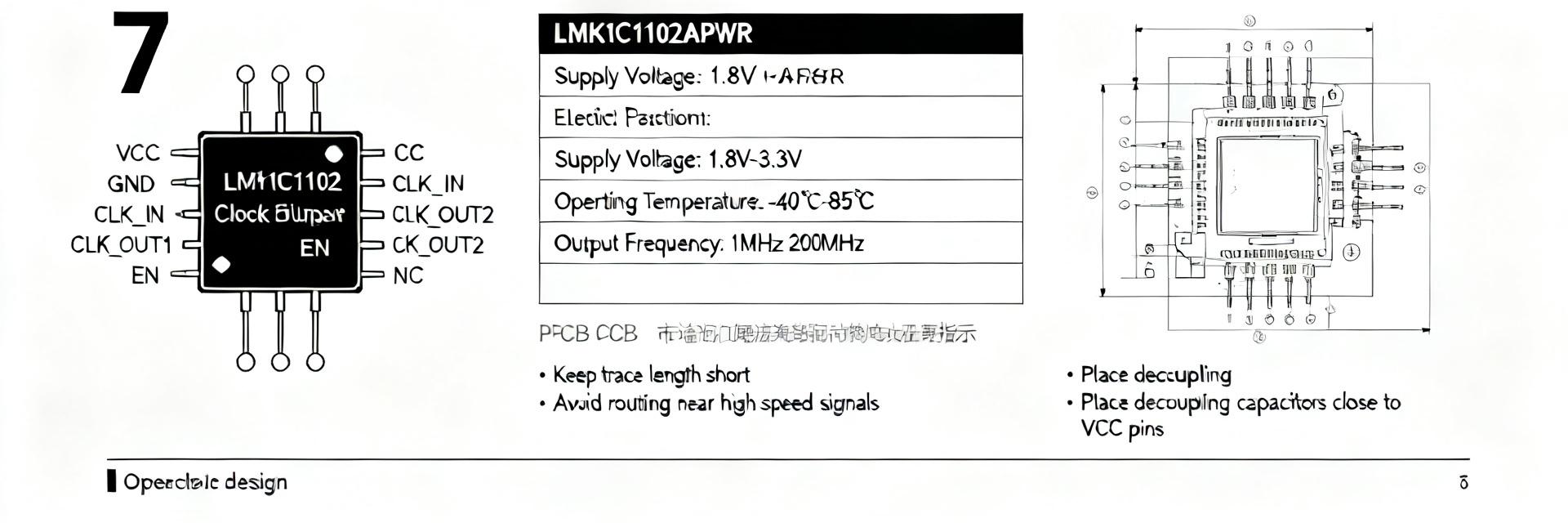
As a high-performance LVCMOS clock buffer/driver, the LMK1C1102APWR features several core advantages, making it an ideal choice for engineers in clock distribution. Its key features include: ultra-low additive jitter (typically <0.1ps), which is critical in high-speed data transmission; support for a wide voltage range of 1.8V, 2.5V, and 3.3V, offering flexibility; and asynchronous operation, simplifying design. These features collectively ensure the purity and stability of the clock signal.
1.1 Ultra-Low Jitter and Wide Voltage Range
The additive jitter of the LMK1C1102APWR is as low as 0.1ps (typical), ensuring that it introduces almost no additional phase noise in high-frequency clock distribution applications, making it an ideal clock source for sensitive devices like FPGAs and ADCs/DACs. Meanwhile, it is compatible with supply voltages of 1.8V, 2.5V, and 3.3V, meaning a single design can span different voltage domains without complex level-shifting circuitry, thereby simplifying the bill of materials (BOM) and PCB design complexity.
1.2 Typical Application Scenarios
The LMK1C1102APWR is widely used in communication systems, data centers, and industrial control fields. For example, in communication base stations, it can be used to distribute reference clocks from phase-locked loops (PLLs); in data center servers, it can provide synchronous clocks for multiple FPGAs and ASICs; in industrial control systems, it can drive multi-channel ADCs for synchronous sampling. These application scenarios all have strict requirements for clock precision, jitter, and drive capability.
2. Detailed Explanation of 7 Key Pin Functions
The LMK1C1102APWR is available in a small package with clearly defined pin functions for easy layout. Understanding the function of each pin is the first step to using the chip correctly. For devices with fewer pins, quickly locating functional pins can greatly shorten the design cycle. The 7 key pins are explained in detail below.
2.1 Functional Pins
CLKIN (Input Clock): This is the input terminal for the clock signal, receiving the LVCMOS clock from an external oscillator or PLL. The integrity and level compatibility of the input signal must be ensured. OE (Output Enable): This pin controls the output state. When OE is high, Y0 and Y1 output active clocks; when OE is low, both outputs enter a high-impedance state. This function is extremely useful during system debugging or power management. Y0, Y1 (Output Clocks): These two pins provide two identical clock outputs, easily driving two independent loads, such as two ADCs or two FPGAs.
2.2 Power and Ground Pins
VDD (Power Supply): Provides the operating voltage for the chip, typically 1.8V, 2.5V, or 3.3V. The datasheet recommends placing 0.1μF and 10μF capacitors next to the VDD pin for decoupling to filter out high-frequency and low-frequency noise on the power line. This is crucial in high-speed designs. GND (Ground): The return path for all currents. In multi-layer PCB design, ensure that the GND pin is connected directly to a large ground plane through short, low-impedance vias, which significantly reduces loop inductance and suppresses noise.
3. Core Electrical Parameters Quick Reference and Interpretation
The core of the datasheet is the electrical parameters table, which defines the performance boundaries of the chip under specific conditions. Correctly interpreting DC and AC characteristics is the basis for timing and design margin analysis. The key parameters are listed below to help you quickly evaluate its performance.
| Parameter Symbol | Parameter Name | Typical Value (3.3V) | Maximum Value (3.3V) | Unit |
|---|---|---|---|---|
| VIH | Input High Voltage | 2.0 | VDD + 0.3 | V |
| VIL | Input Low Voltage | 0.8 | 0.8 | V |
| tpd | Propagation Delay | 1.9 | 2.5 | ns |
| tr / tf | Output Rise/Fall Time (20% - 80%) | 0.8 | 1.2 | ns |
| tsk(o) | Output Skew (same device) | 30 | 150 | ps |
| fmax | Maximum Operating Frequency | - | 250 | MHz |
3.1 DC Characteristics
Key DC parameters include input high/low voltage (VIH/VIL), output high/low voltage (VOH/VOL), and supply current (IDD). For example, under a 3.3V supply, the typical VIH is 2.0V and typical VIL is 0.8V. This means the input signal must be higher than 2.0V to be recognized as high level. The typical IDD is only a few milliamperes, reflecting its low-power characteristics. Understanding these parameters ensures correct logic level matching between stages.
3.2 AC Characteristics
AC parameters are key to evaluating the speed performance of the chip. Main parameters include propagation delay (tpd), output rise/fall time (tr/tf), and maximum clock frequency (fmax). For example, at 3.3V, typical tpd might be 2.5ns, and typical tr/tf might be 1.0ns. These values directly determine the timing margin of the system. In high-speed designs, these delays must be included in timing analysis to ensure that the setup and hold times of all devices are met.
4. PCB Layout Guide Based on Datasheet
Good PCB layout is the physical foundation for realizing chip performance. The layout recommendations in the datasheet are not optional but are proven best practices. Following these guidelines avoids many common signal integrity issues in high-frequency designs.
4.1 Pin Routing and Impedance Control
For critical signals such as CLKIN, Y0, and Y1, 50Ω impedance-controlled routing is recommended. Traces should be as short and straight as possible, avoiding 90-degree sharp bends to reduce signal reflections. At the same time, try to keep the trace lengths of Y0 and Y1 equal to minimize clock skew. Minimize the number of vias, as each via introduces parasitic inductance and capacitance, affecting signal quality.
4.2 Power and Ground Plane Design
Providing a stable, low-noise power supply to the VDD pin is critical. In addition to decoupling capacitors, a complete power plane should be used to supply power instead of simple traces. The GND pin must connect directly to a solid ground plane through multiple vias. Never split the ground plane under clock signals, as ground plane discontinuities cause impedance mismatches and severe signal reflections, which degrade clock jitter.
Key Summary
- Core Function Quick Reference: The LMK1C1102APWR is an LVCMOS clock buffer integrating ultra-low jitter, wide voltage range, and asynchronous enable functions for high-quality clock distribution.
- Pin Function Analysis: Understanding the functions of the 7 key pins, including CLKIN, OE, Y0/Y1, VDD, and GND, is the basis for correctly applying this device.
- Electrical Parameter Interpretation: Mastering the DC and AC characteristic parameters (VIH, VIL, tpd, tr, etc.) helps engineers accurately evaluate timing margins and verify design reliability.
FAQ
What is the most important parameter in the LMK1C1102APWR datasheet?
For high-speed designs, the most important parameters are additive jitter and propagation delay (tpd). Additive jitter determines the purity of the clock signal, directly affecting the system's signal-to-noise ratio; propagation delay determines the time offset of the signal along the path, which is a critical input for timing analysis.
How to select decoupling capacitors for LMK1C1102APWR?
The datasheet recommends placing a 0.1μF high-frequency ceramic capacitor and a 10μF tantalum or multilayer ceramic capacitor next to the VDD pin. The 0.1μF capacitor should be placed as close as possible to the VDD pin to filter out high-frequency noise; the 10μF capacitor is used to smooth low-frequency fluctuations and store energy. Both combined provide effective decoupling over a wide frequency range.
If the output enable (OE) pin is left floating, what will be the consequences?
The OE pin usually has a weak internal pull-up or pull-down resistor, but to ensure determinism, it is recommended not to leave it floating. Floating can lead to unstable input states, causing the output to enter an indeterminate state or generate unexpected glitches. Best practice is to connect it to VDD (when active) via a pull-up resistor or to GND via a pull-down resistor.
Can the LMK1C1102APWR be used to drive long-distance clock signals?
Although it has driving capability, it is not recommended to use it to directly drive backplanes inside a chassis or long traces exceeding several inches. Long traces create severe impedance discontinuities and attenuation, leading to signal degradation. For long-distance transmission, buffers or differential signaling converters should be used.
In a multi-layer PCB, can other signal lines be routed under the LMK1C1102APWR?
It is highly discouraged to route any high-speed or sensitive signal lines on PCB layers directly underneath the clock buffer. The area below the chip should serve as a clean reference ground plane. This minimizes signal coupling and crosstalk, ensuring clock signal integrity. All unrelated traces should avoid this area.