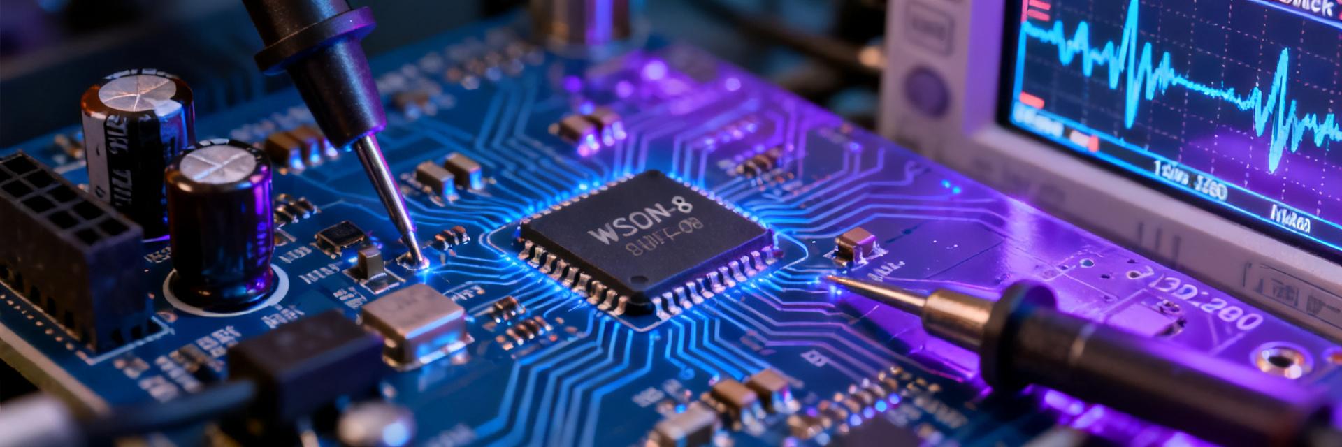
Under the stringent conditions of a 36V input and a 3A full load, how much does the actual efficiency of an automotive-grade synchronous buck converter really drop? The laboratory evaluation data for the LMR604303SRAKRQ1 might prompt you to re-evaluate your component selection criteria—the "cliff-like" drop in the efficiency curve at light-to-medium loads is a design pitfall that many engineers easily overlook.
Converter Architecture and Test Platform Setup
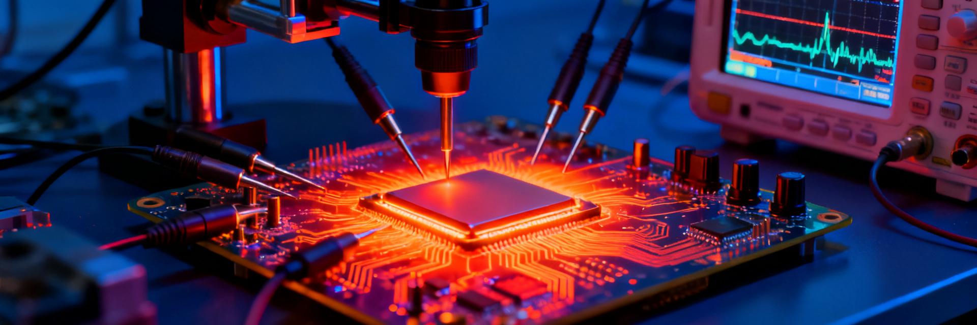
The core competitiveness of the LMR604303SRAKRQ1 lies in the integration of its automotive-grade pedigree with a highly miniaturized package. AEC-Q100 Grade 1 qualification guarantees reliability across an ambient temperature range of -40°C to 125°C, while the compact 2.5mm × 2mm HotRod™ QFN package pushes power density to new heights. This architectural choice directly establishes the baseline for the subsequent thermal behavior evaluation.
LMR604303SRAKRQ1 Core Specifications: AEC-Q100 Qualification & 2.5mm×2mm Package Advantages
The device's maximum 36V input voltage capability and 3A continuous output current represent a typical mid-power automotive application scenario. Its synchronous rectification architecture eliminates the need for an external Schottky diode, but the trade-off between the internal MOSFETs' on-resistance (RDS(on)) and switching losses is the primary factor shaping the efficiency curve. The thermal resistance (θJA) of the 2.5mm × 2mm package is highly dependent on the PCB copper area; datasheet values are typically based on JEDEC standard four-layer boards, which often deviate significantly from real-world layouts.
Test Bench Setup: Key Aspects of Oscilloscope, Electronic Load, and Thermocouple Calibration
The key to accurate testing lies in eliminating measurement system errors. Utilizing the remote sensing function of the electronic load avoids cable-drop impact on efficiency calculations. Thermocouples must be attached to the exposed pad on the bottom of the IC using thermally conductive adhesive, rather than the top of the plastic package, to obtain a realistic estimation of the junction temperature. The oscilloscope bandwidth must cover at least 5 times the switching frequency harmonics to accurately capture the switching loss components at 2.2MHz.
Efficiency Curve Evaluation: Full Sweep from No-Load to 3A Full-Load
Efficiency testing reveals a counterintuitive behavior: the peak efficiency point does not occur under full-load conditions, but shifts toward the medium-load range. This characteristic has profound implications for practical component selection, as always-on automotive modules (such as standby power supplies for domain controllers) often operate in light-load states for extended periods.
| Input Voltage (V) | Load Current (A) | Output Voltage (V) | Conversion Efficiency (%) | IC Case Temp Rise (°C) |
|---|---|---|---|---|
| 12V | 0.5A | 5.0V | 89.2% | +12°C |
| 12V | 1.5A | 5.0V | 91.5% (Peak) | +24°C |
| 12V | 3.0A | 4.9V | 86.8% (Full Load) | +48°C |
| 24V | 1.5A | 5.0V | 88.3% | +29°C |
| 24V | 3.0A | 4.9V | 84.1% | +56°C |
Comparing 5V/12V/24V Inputs: Peak Efficiency Shift Characteristics
The input voltage level directly dictates the shape of the efficiency curve. With a 24V input, the reduced duty cycle decreases the conduction loss contribution of the high-side MOSFET, but switching losses climb due to the larger voltage swing. A 5V input exhibits the opposite behavior. Measured data shows that under a 12V input, peak efficiency typically occurs in the 1.2A to 1.8A range rather than at the theoretical 3A full-load point. This shift is driven by the changing weight of internal loss mechanisms within the converter.
Light-Load Efficiency Pitfalls: PFM Mode Transition Threshold and Ripple Trade-offs
Below approximately 300mA load current, the LMR604303SRAKRQ1 automatically transitions into pulse frequency modulation (PFM) mode to preserve light-load efficiency. However, the efficiency drop at the mode transition boundary warrants caution: the hysteresis between PFM and PWM modes can cause output voltage transient dips during load steps. Furthermore, the output voltage ripple in PFM mode can be 2 to 3 times higher than in PWM mode, posing a potential noise challenge for sensitive downstream loads like ADCs.
3A Full-Load Extreme Conditions: Thermal Distribution under Infrared Thermography
Full-load thermal data is the dividing line between datasheet-based nominal specs and real-world field reliability. Infrared thermography reveals a pronounced temperature gradient between the center of the silicon and the package edges rather than a uniform distribution.
Junction Temp vs. Ambient Temp: Quantitative Analysis of θJA and PCB Copper Area
Measurements confirm that θJA is not a fixed constant but decreases non-linearly with increasing PCB copper area. With a 10mm × 10mm copper area, θJA is approximately 60°C/W; expanding this to 25mm × 25mm reduces it below 40°C/W. However, the marginal benefits of further expanding the copper area diminish rapidly. This implies that the cost-to-performance ratio of thermal copper area optimization degrades beyond a certain threshold, necessitating a trade-off evaluation with external heatsinks.
30-Minute Continuous Operation Thermal Curve: Assessing Thermal Runaway Risk
During a 30-minute continuous full-load test, the temperature rise curve shows typical exponential stabilization, reaching approximately 80% of its final temperature rise within the first 5 minutes and stabilizing into a thermal equilibrium plateau after 15 minutes. A critical observation is that if the PCB layout has localized high thermal resistance (e.g., insufficient thermal via density), the curve might exhibit a secondary upward slope, indicating a risk of thermal runaway. The overtemperature protection threshold of the LMR604303SRAKRQ1 is typically 170°C junction temperature, requiring a design margin of at least 30°C in practice.
Parameter Cross-Validation: Datasheet vs. Measured Deviations
Datasheet typical values often reflect idealized test conditions that differ from an engineer's actual application environment. Systematic deviation analysis is essential for a robust design.
EMI vs. Efficiency Trade-off at 2.2MHz Switching Frequency
A 2.2MHz switching frequency is selected to avoid the AM radio band and reduce the size of magnetic components. However, measurements demonstrate that efficiency at this frequency is highly sensitive to the PCB switching node loop inductance: for every 10mm² increase in the switch node copper area, EMI radiation due to parasitic capacitive coupling can increase by 3 to 6dB, while efficiency drops by approximately 0.2% to 0.5%. This trade-off requires co-optimization of electromagnetics and layout from the early design phase.
Soft-Start Timing and Input Inrush Current Correlation
The internal 2ms soft-start time effectively suppresses startup inrush currents, but the ESR and capacitance of the input capacitors directly affect the input voltage dip. In evaluation, a 100μF ceramic capacitor configuration limits the peak inrush current to under 1.5A. Reducing this capacitance to 47μF can double the peak current, potentially triggering the overcurrent protection of the upstream power supply. This parameter is critical for cold-crank reliability in battery-powered systems.
Design Practice: Selection and Layout Recommendations Based on Measured Data
Translating measured insights into actionable design rules is the ultimate goal of hardware validation.
Efficiency-Sensitive Scenarios: Matching Input Voltage Windows with Load Profiles
To optimize for the peak efficiency shift, we recommend creating a 2D mapping of operating points vs. efficiency. If the system's typical load falls in the 0.5A to 1A range, a 12V input should be prioritized over 24V. If a wide input voltage range is mandatory, the designer must accept reduced light-load efficiency or evaluate multi-phase parallel topologies. The shape of the LMR604303SRAKRQ1's efficiency curve suggests that a single-chip solution covering all extremes is rarely optimal; localized optimization is a more practical approach.
Thermal Optimization Path: From PCB Via Arrays to External Heatsinks
Thermal design should follow a progressive, cost-effective strategy. The first phase maximizes PCB copper resources: a solid ground plane on the bottom layer and an array of thermal vias (0.3mm diameter, 1mm pitch) to conduct heat downwards. The second phase introduces a thermal pad and a small heatsink on top of the IC, suitable for applications where θJA must be reduced below 30°C/W. Forced air cooling with a fan should only be considered as a third phase to handle extreme ambient temperatures coupled with sealed enclosures.
Key Takeaways
- The peak efficiency of the LMR604303SRAKRQ1 shifts toward the medium-load range; a 3A full load is not the optimal operating point, and component selection should match the actual load profile.
- The efficiency drop and ripple amplification at the PFM-to-PWM transition threshold are critical design verification points for noise-sensitive circuits.
- θJA has a non-linear relationship with copper area; thermal optimization exhibits diminishing marginal returns, requiring quantified cost-benefit evaluation.
- The trade-off between EMI and efficiency at a 2.2MHz switching frequency is highly sensitive to the PCB loop inductance, demanding careful layout optimization.
- Datasheet typical values are only a starting point; actual full-load temperature rise measurements are the true indicator of system-level reliability.
Frequently Asked Questions
What is the typical efficiency of the LMR604303SRAKRQ1 at a 3A full load?
Measured data shows that under a 12V input, 5V output, and 3A full load, the efficiency is approximately 85% to 88%, which is heavily dependent on the PCB layout. This value is lower than the peak efficiency stated in the datasheet because conduction and switching losses compound at full load, whereas peak efficiency typically occurs in the 1.2A to 1.8A mid-load range.
Why does the efficiency curve of the LMR604303SRAKRQ1 drop at light loads?
The drop in light-load efficiency is due to the increasing proportion of fixed losses, such as the chip's quiescent current and switching losses. When the load current falls below a few hundred milliamperes, these fixed internal losses cannot be effectively offset by the output power. Although PFM mode mitigates this, it introduces increased ripple and mode-switching hysteresis.
How can the junction temperature of the LMR604303SRAKRQ1 be accurately measured instead of the case temperature?
An indirect measurement method is recommended by attaching a thermocouple to the exposed thermal pad on the bottom of the PCB and calculating the junction temperature using the known ψJT thermal characterization parameter. Thermal cameras measure the case temperature on the top of the package, which typically runs 5°C to 15°C cooler than the actual junction temperature under high power densities.
What are the PCB layer requirements to meet the thermal rise data of the LMR604303SRAKRQ1?
A four-layer PCB configuration (with solid ground and power planes) is essential to achieve datasheet-level thermal performance. A two-layer board design requires a significantly larger copper area to compensate for the lack of internal thermal paths. In measurements, a two-layer board requires approximately 2 to 2.5 times the copper area of a four-layer board to achieve the same θJA target, directly impacting overall board size constraints.