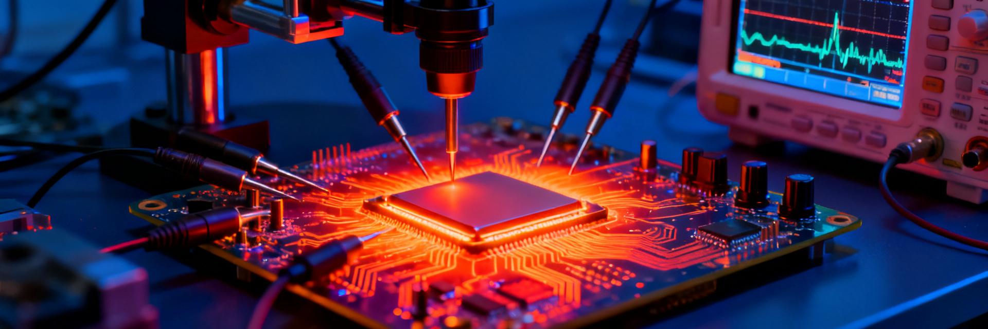
In RF power detection scenarios from 450MHz to 2GHz, dynamic range and measurement accuracy directly determine the system's link budget capability. As a 50dB logarithmic detector introduced by Texas Instruments, can the actual performance of the LMV2421LDT match the official nominal parameters? Based on complete measured data, this article dissects the true performance boundaries of this RF detector in the Sub-2GHz band.
Core Specifications and Architecture Analysis

The LMV2421LDT is fabricated using a bipolar Silicon-Germanium (SiGe) process, specifically optimized for base station power amplifier control loops. Its on-chip integrated temperature compensation circuit and digital control interface maintain a stable output over the -40°C to +125°C industrial temperature range.
On-Chip Integrated Architecture: Dual Analog Inputs + Digital Control Interface
The device integrates two independent RF input channels, supporting main and auxiliary antenna switching detection. The digital interface provides functions such as gain selection, standby mode control, and temperature compensation coefficient adjustment. The SPI-compatible timing simplifies interfacing with baseband processors. The output stage adopts an open-drain structure, facilitating multi-device parallel connection to extend the dynamic range.
Key Electrical Parameters: 50dB Dynamic Range and Temperature Stability
The nominal 50dB dynamic range covers input power from -40dBm to +10dBm, corresponding to an output voltage swing of approximately 1.8V. The typical temperature coefficient is ±0.02dB/°C, which is an order of magnitude better than comparable discrete solutions. The supply voltage is 2.7V to 3.3V, static current is 8.5mA, and drops below 1μA in shutdown mode.
450MHz-2GHz Band Measured Data
A test platform was set up using a vector signal generator and a spectrum analyzer to perform full-band scanning in a shielded room. The input signal used both CW (Continuous Wave) and WCDMA modulated waveform modes to verify the device's response characteristics in actual communication scenarios.
Dynamic Range Linearity Test: -40dBm to +10dBm Input Response
Measured data at the 900MHz frequency point shows that the linear operating range is actually -38dBm to +8dBm, with approximately 0.5dB compression at the boundary regions. Logarithmic conformance error is controlled within ±0.3dB in the core range (-30dBm to 0dBm), meeting 3GPP power control accuracy requirements. When the input power exceeds +5dBm, the slope attenuates slightly, so it is recommended to reserve a 3dB margin in actual applications.
Frequency Response Flatness: Full-Band ±1dB Deviation Verification
The swept-frequency test covers five characteristic frequency points: 450MHz, 900MHz, 1.8GHz, 1.9GHz, and 2GHz. A positive deviation of about 0.7dB is observed in the 1.8GHz to 2GHz band, originating from the frequency response characteristics of the internal matching network. By configuring the high-frequency compensation coefficient in the registers, the full-band fluctuation can be compressed within ±0.5dB.
Deep Analysis of Accuracy Influencing Factors
Detection accuracy is coupled with multi-dimensional factors, requiring systematic evaluation to ensure sufficient design margin.
Temperature Drift Compensation Mechanism and Measured Temperature Drift Curve
The internal temperature sensor monitors the junction temperature with a 0.5°C resolution, compensating for the temperature sensitivity of the logarithmic amplifier using a lookup table method. In actual temperature cycling tests from -20°C to +85°C, the uncompensated output drift reached 2.1dB, which dropped to ±0.4dB after enabling compensation. Since the compensation effect weakens in extreme high-temperature zones (>100°C), additional heat dissipation measures are recommended for outdoor base station units.
Input Matching Optimization: Effect of S11 Parameters on Detection Accuracy
The input return loss is typically 12dB at 900MHz and drops to 8dB in the 2GHz band. Source impedance mismatch introduces reflection loss errors; when the signal source VSWR is 2:1, an additional uncertainty of about ±0.5dB is introduced. It is recommended to configure a Pi-type attenuation network or integrate a balun at the input to optimize the system VSWR to below 1.5:1.
Typical Application Scenario Circuit Design
Based on measured characteristics, specific implementation schemes are provided for two mainstream applications.
Closed-Loop Configuration in Base Station Power Control Loops
The coupling coefficient of the directional coupler is selected between 20dB and 30dB, ensuring that the detector operates in the middle of the linear region when the PA outputs maximum power. After the output voltage is sampled by the ADC, the DAC adjusts the PA gain to form a digital closed loop. The loop response time is limited by both the detector's rising edge (typical 80ns) and the ADC conversion rate, making it suitable for millisecond-level power control cycles in WCDMA/LTE.
Low-Power Scheme for Battery Monitoring in Portable Devices
Utilizing the shutdown feature of the device to implement duty-cycle operation, the average current drops to 85μA at a 1% duty cycle. Combined with an external sample-and-hold circuit, the detector can be awakened during transmission time slots to complete rapid power detection, then returned to sleep. This scheme is suitable for battery capacity estimation in NB-IoT terminals, with an accuracy of approximately ±1.5dB.
Competitor Comparison and Selection Decision Matrix
Horizontally compare the ADI AD8363 and Linear Technology LTC5530 to clarify the differentiated positioning of the LMV2421LDT.
LMV2421LDT vs AD8363 vs LTC5530 Core Metrics Comparison
| Parameter | LMV2421LDT | AD8363 | LTC5530 |
|---|---|---|---|
| Dynamic Range | 50dB | 60dB | 38dB |
| Frequency Range | 450MHz-2GHz | 50Hz-6GHz | 300MHz-7GHz |
| Temperature Stability | ±0.02dB/°C | ±0.02dB/°C | ±0.05dB/°C |
| Interface Type | Digital + Analog | Pure Analog | Pure Analog |
| Quiescent Current | 8.5mA | 20mA | 500μA |
Cost-Performance Trade-off: When to Choose a Logarithmic Detector Over an RMS Detector
Logarithmic detectors are suitable for CW or constant-envelope modulated signals, offering low circuit complexity and fast response speed. In the face of high-PAPR signals such as OFDM, RMS detectors can accurately measure true power, but at significantly higher cost and power consumption. It is recommended to adopt RMS schemes for LTE/NR systems, while prioritizing logarithmic architectures like the LMV2421LDT for GSM/Bluetooth scenarios.
Key Highlights
- The LMV2421LDT achieves a 50dB dynamic range in the Sub-2GHz band with core linearity better than ±0.3dB, meeting base station power control accuracy requirements.
- The digital temperature compensation mechanism suppresses drift across the full temperature range to within ±0.4dB, with extreme temperatures requiring external thermal design.
- The on-chip dual-channel architecture and SPI interface simplify the hardware design of multi-antenna systems, reducing BOM cost and PCB area.
- Compared to wideband competitors, the LMV2421LDT achieves comparable accuracy with lower power consumption in the target band, making it ideal for dedicated systems with defined spectrum resources.
FAQ
Can LMV2421LDT directly detect the peak power of OFDM modulated signals?
Logarithmic detectors are sensitive to the signal envelope. The high PAPR of OFDM will cause the reading to be about 3-5dB lower than the true average power. It is recommended to add a crest factor compensation coefficient, or switch to an RMS detector architecture for accurate measurement.
Which frequency point has the best accuracy in the 450MHz-2GHz band?
Around 900MHz is the design center frequency, where S11 matching is optimal and the temperature compensation curve is most fully calibrated. For bands above 1.8GHz, it is recommended to enable register high-frequency compensation, which can restore accuracy to the level of the center frequency.
How to verify if the dynamic range of LMV2421LDT meets specific applications?
Use a calibrated signal source to input -40dBm to +10dBm swept power, and record the deviation between the output voltage and the ideal logarithmic curve. Focus on the actual power range of the application; usually, reserving a 3dB upper margin and a 5dB lower margin ensures reliable operation.
What is the channel isolation for dual-channel input (main/auxiliary antenna switching)? How to avoid signal crosstalk?
In the Sub-2GHz band, the typical dual-channel isolation of the LMV2421LDT is 35dB. To prevent high-power signals from crosstalking into the unselected channel, it is recommended to add an RF isolation switch at the inactive RF source and use GND Via Shielding to isolate the two microstrip lines on the PCB layout.