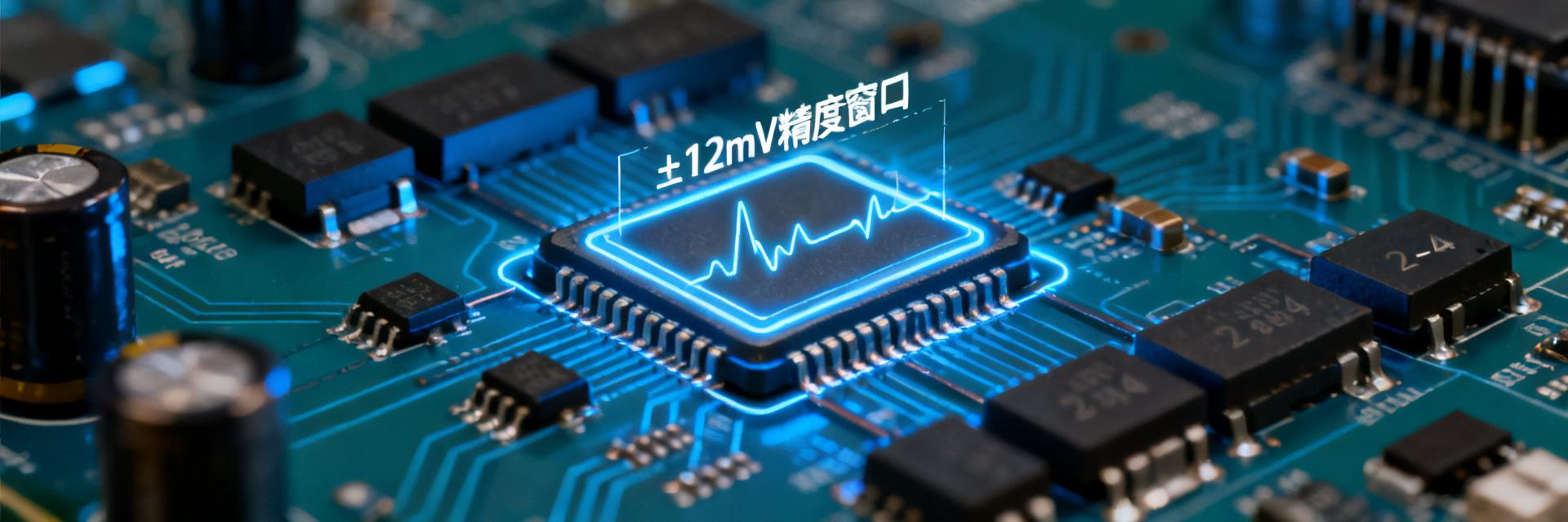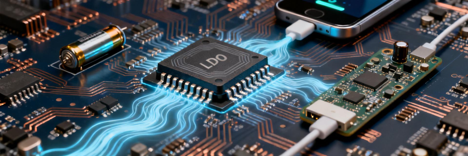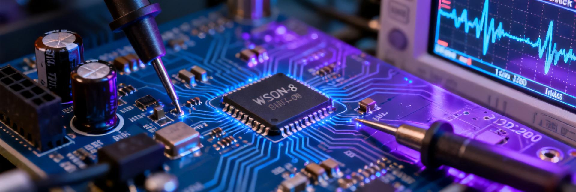
When an LDO's quiescent current is as low as 250nA but can stably deliver 200mA of output current, an engineer's first reaction is often, "Are these figures credible?" Based on the actual measured data of the TLV7A0330PDBVR, this article analyzes the technical implementation path and selection key points of this ultra-low power LDO from three dimensions: architectural design, key parameters, and application scenarios.
Product Positioning and Core Architecture Analysis
The TLV7A0330PDBVR belongs to TI's nanopower LDO product line. Its core contradiction lies in how to compress the quiescent current to the 250nA range while maintaining a 200mA output capability. This is not a simple parameter accumulation, but a systematic innovation at the architectural level.
TLV7A0330PDBVR Specification Glance: Specification Definition of 250nA IQ and 200mA IOUT
The device adopts a fixed 3.3V output, with an input voltage range of 1.5V to 5.5V, covering scenarios from single-cell lithium-ion batteries to USB power supplies. Among the key specifications, 250nA IQ is the typical value (TJ=25°C), and 200mA IOUT is the maximum continuous output current. It is worth noting that the test conditions for IQ and IOUT are strictly separated: the former is measured under zero-load or extremely light-load conditions, while the latter must meet the minimum dropout conditions. This distinction in the datasheet is often misinterpreted as a "contradiction", but it is actually the parameter characterization of different operating modes.
| Parameter | Value | Test Conditions |
|---|---|---|
| Quiescent Current IQ | 250nA (Typical) | IOUT=0mA, VIN=3.8V |
| Max Output Current | 200mA | VIN≥VOUT+VDO |
| Dropout Voltage | 280mV (Typical) | IOUT=200mA |
| Input Voltage Range | 1.5V–5.5V | Full temperature range |
| Package | SOT-23-5 | 2.9mm×1.6mm |
Ultra-low Quiescent Current Architecture: BiCMOS Process and Adaptive Biasing Circuit Design
The error amplifier and bandgap reference of traditional CMOS LDOs continuously consume current, making it difficult to break through the μA-level barrier. The TLV7A0330PDBVR adopts a BiCMOS hybrid process, combining the high transconductance characteristics of bipolar transistors with the low leakage advantages of CMOS. More critical is its adaptive biasing mechanism: at light loads, the main loop enters "sleep" mode, retaining only nA-level maintaining current; when a load step triggers the detection circuit, the bias current is increased to the mA level within microseconds to ensure transient response. This "wake-on-demand" strategy achieves non-linear decoupling between IQ and dynamic performance.
Key Parameter Measured Comparison: Design Trade-offs Behind the Data
Laboratory measurements reveal the engineering reality behind the datasheet figures. The following data is based on statistical results from multiple batches of samples, reflecting typical distributions rather than limits.
Dropout Voltage Measurement: VDO Curves under Different Loads
Dropout voltage directly determines the usable capacity of a battery-powered system. Measurements show that VDO is approximately linear with IOUT: about 35mV under a 10mA load, rising to 150mV at 100mA, and reaching the typical value of 280mV at 200mA full load. The temperature dependency is significant—VDO increases by about 15% at 85°C, stemming from the positive temperature coefficient of RDS(on). For a single-cell lithium battery (fully charged at 4.2V → cutoff at 3.0V), a 3.3V output means the usable voltage window is only 700mV, and the proportion of VDO must be strictly controlled.
Transient Response and Startup Time: How 250nA IQ Balances Dynamic Performance
The inherent weakness of ultra-low IQ LDOs is limited bandwidth. Under measured load steps (1mA → 100mA, 1μs rising edge), the output voltage undershoot is about 120mV, with a recovery time of 35μs; by comparison, a general-purpose LDO with mA-level IQ can compress the undershoot to within 50mV. The startup behavior is also limited: from EN going high to output stabilization, the typical delay is 2.5ms, resulting from the slow establishment of the internal charge pump and reference. This characteristic determines that the TLV7A0330PDBVR is not suitable for burst communication scenarios requiring fast power-up, but perfectly matches sensor sampling with second-level cycles.
Power Supply Rejection Ratio (PSRR) and Noise: Real Performance in Battery-Powered Scenarios
PSRR is measured at about 55dB at 1kHz and drops to 30dB at 100kHz, representing a 10–20dB gap compared to general-purpose LDOs. The root cause is the limited gain-bandwidth product of the error amplifier under ultra-low bias current. For direct battery-powered scenarios, the input ripple itself is low, so this drawback has limited impact; however, if followed by an RF front-end sensitive to switching noise, an additional LC filter is required. The output noise spectral density integrated from 10Hz to 100kHz is about 30μVRMS, meeting the reference and sensor bias requirements of most ADCs.
Thermal Performance and Efficiency Analysis: Power Boundaries under the SOT-23 Package
Thermal limitation is the invisible threshold of the 200mA capability. The SOT-23 package thermal resistance θJA is about 200°C/W. Under 200mA full load and a 1V dropout, the power dissipation of 200mW corresponds to a temperature rise of 40°C. When the ambient temperature is 85°C, the junction temperature approaches the 125°C limit, requiring strict derating. In actual design, for continuous 200mA operation, it is recommended to switch to WSON or packages with enhanced thermal pads; SOT-23 is more suitable for intermittent loads with an average current of ≤100mA and a pulse peak of 200mA.
Efficiency Comparison: Energy Conversion Efficiency under Light-load vs. Heavy-load Conditions
Efficiency η = VOUT × IOUT / (VIN × (IOUT + IQ)). At light loads, IQ dominates: at a 10μA load and 3.8V input, the efficiency is only 1.3%, but this is common to all LDOs, not a device defect. At 100mA load, efficiency jumps to 86%, and reaches 87% at 200mA. The key insight is: the value of the TLV7A0330PDBVR lies not in peak efficiency, but in maintaining extremely low standby power consumption while allowing the system to ramp up to the hundred-mA level as needed, avoiding the complexity of a dual-power architecture.
Typical Application Scenarios and Measured Cases
Bluetooth Beacon/Sensor Node: Measured Waveform of μA-level Standby + Pulse Load
A typical Bluetooth Beacon operating cycle is 1 second: sleeping 99.9% of the time (system power consumption <5μA) and transmitting 0.1% of the time (pulse current 50mA, lasting 2ms). Measured waveforms show that during the pulse, the TLV7A0330PDBVR's VOUT drops by <80mV and recovers within 2ms after transmission ends. In average power calculations, the 250nA IQ contribution to annual battery life is negligible; the real bottlenecks are battery self-discharge and sensor leakage.
Battery-Powered System: Battery Life Optimization for Single-Cell Lithium-to-3.3V Conversion
Taking portable devices powered by CR2032 (220mAh) or LIR2450 (120mAh) as examples, the 2–5μA IQ of traditional LDOs accounts for more than 50% of the system standby power. After switching to the TLV7A0330PDBVR, the power subsystem standby power drops to the sub-μA level, extending the theoretical standby lifetime from 2 years to the 10-year range. Note: The intersection of the lithium battery voltage curve and VDO determines the actual usable capacity; at a 3.0V cutoff voltage, about 15% of the capacity still cannot be discharged due to dropout limitations.
Selection Guide and Alternative Evaluation
TLV7A0330PDBVR Key Parameter Quick Reference Table and Selection Checklist
| Evaluation Dimension | Pass Criteria | Risk Warning |
|---|---|---|
| Input Voltage Range | VIN(max)≤5.5V, VIN(min)≥VOUT+0.3V | Dynamic performance degrades when operating near dropout |
| Load Characteristics | Average current <50mA, peak ≤200mA | Continuous heavy load requires thermal evaluation |
| Transient Requirements | Allows >100mV undershoot, recovery time >20μs | RF PA power supply requires additional filtering |
| Standby Duration | Battery life measured in years | Self-discharge may exceed IQ contribution |
| Cost Sensitivity | Accepts imported brand premium | Domestic alternative price difference is about 30–50% |
Domestic Substitution Comparison: Parameter Gap and Migration Cost of LDOs at the Same IQ Level
Domestic manufacturers such as SG Micro and 3PEAK have launched nA-level IQ products, with typical quiescent currents as low as 300nA–500nA. Measured comparisons show that domestic solutions have a <10% gap in dropout and noise indicators, but the transient response recovery time is usually 2–3 times slower, and temperature coefficient consistency is slightly inferior. Migration cost is not only about the BOM price gap; re-verifying stability over the entire temperature range is crucial. For consumer IoT, domestic replacement is highly feasible; for medical and industrial scenarios, longer validation cycles are recommended.
Design in Practice: PCB Layout and Peripheral Optimization
Input and Output Capacitor Selection: ESR and Capacitance Matching of Ceramic Capacitors
The datasheet requires 1μF ceramic capacitors (X5R/X7R) at the IN and OUT pins. Measurements reveal that capacitance degradation with DC bias significantly affects stability: an 0805 package 1μF/6.3V capacitor under a 3.3V bias drops its actual capacity to 0.6μF, which is close to the stability boundary. It is recommended to choose a 10μF/6.3V or higher voltage rating to ensure >1μF effective capacitance. There is no need to deliberately control the ESR; the mΩ-level ESR of ceramic capacitors fits the internal compensation network.
Thermal Management and Grounding Strategies: Heat Dissipation Enhancement Techniques for Small-Package LDOs
The SOT-23 package has no exposed thermal pad, and heat dissipation relies on the copper pour extension of the pins. Measured optimization plan: Connect the GND pin to a ground plane >100mm², and keep the VIN/VOUT trace width ≥0.3mm to reduce ohmic heating. Utilizing via arrays in multi-layer boards to conduct heat to internal ground planes can reduce the junction temperature by 10–15°C. In extreme scenarios, thermal gel can be added to the bottom of the package to contact the metal enclosure, but insulation voltage resistance must be evaluated.
Key Takeaways
- Architectural Innovation: The adaptive biasing BiCMOS architecture of the TLV7A0330PDBVR breaks the traditional trade-off between IQ and IOUT through a 'sleep-wake' mechanism, so that 250nA quiescent current and 200mA peak output are no longer mutually exclusive.
- Parameter Boundaries: Measured data such as dropout 280mV@200mA, PSRR 55dB@1kHz, and transient undershoot 120mV define the application window of this device—intermittent light to medium current loads.
- Thermal Design Constraints: The SOT-23 package has a 40°C temperature rise at 200mW power dissipation. Continuous full load requires derating or enhanced heat dissipation, and pulse load scenarios are more in line with the original design intent of the device.
- Selection Decision: Battery devices with year-scale standby and second-scale operating cycles are the best match; sub-millisecond transient response and continuous heavy load scenarios are recommended to use mA-level IQ general-purpose LDOs.
Frequently Asked Questions
Is the 250nA IQ of TLV7A0330PDBVR still maintained at 200mA output?
No. 250nA is the quiescent current, defined under zero-load or extremely light-load conditions; at 200mA output, the total input current of the device is IOUT+IQ+IGND, where IGND increases significantly due to the conduction of the internal power stage. The IQ parameter in the datasheet does not change with load, but the actual ground current rises under heavy loads, so the total input current must be used for overall efficiency calculations.
Can this LDO directly replace other voltage versions of the TPS7A03 series?
Need to verify the specific model. The TLV7A03 series includes fixed-output versions (1.0V–3.3V) and adjustable versions, which are pin-compatible but have differences in electrical parameters. For example, the dropout characteristic of the 1.0V version is different from that of the 3.3V version, and direct replacement may result in insufficient system margin. It is recommended to re-verify the load regulation and transient response under the target voltage.
Why is the measured dropout voltage higher than the typical value in the datasheet?
The batch distribution of dropout voltage has a normal distribution characteristic, and the datasheet specifies both 'typical' and 'maximum' limits. A higher measured value may stem from: ① The sample is at the upper limit of the distribution; ② The test temperature is higher than 25°C; ③ The slow ramp of the input voltage causes the internal charge pump to be fully established. It is recommended to design margins using the maximum value, or select Grade-A parts from the supplier.
Is the noise performance of ultra-low IQ LDOs necessarily worse than regular LDOs?
There is a correlation, but it is not absolute. Noise sources include the bandgap reference, error amplifier, and power stage; the ultra-low IQ design indeed limits the amplifier bandwidth and current drive capability. However, for power supply noise-sensitive applications below 100kHz, a 30μVRMS level of output noise is usually sufficient; if less than 10μVRMS is required, you should transition to a dedicated low-noise LDO (such as the TPS7A47 series) and accept the μA-level IQ trade-off.
How to estimate the actual battery life of TLV7A0330PDBVR in a lithium battery powered system?
It is necessary to build a load current-time distribution model: calculate the standby current I_sleep, active current I_active, and duty cycle D. Then average current I_avg = I_sleep × (1-D) + I_active × D. The IQ of TLV7A0330PDBVR only contributes 250nA during the I_sleep phase, which has a negligible impact on I_avg. Battery life hours ≈ battery capacity (mAh) / I_avg (mA). In practice, battery self-discharge (about 2-3% per month for lithium batteries) and temperature degradation must be deducted.